Thursday, August 30, 2018

Apple vs Samsung in ALS and Proximity Sensors

SystemPlus Consulting compares ambient light sensors (ALS) and proximity sensors design in several generations of Apple and Samsung smartphones: Samsung Galaxy S7, S8, and S9 and Apple iPhone 7, 8, and X:

"Samsung has chosen to combine the two sensors in a single component, whereas Apple made the choice to keep them separate. Over the years, Samsung has improved the performance without changing its packaging footprint. Apple has kept the same supplier, STMicroelectronics, for its proximity sensor. However it has added features to each new generation, as in the latest the iPhone X, where the proximity sensor is combined with a flood illuminator. In this new iPhone the ambient light sensor is still supplied by ams, but has a multi-spectral feature."

Samsung Galaxy S9 combined proximity/ALS sensor
Apple iPhoe X multi-spectral ALS

Wednesday, August 29, 2018

e2v Announces Optimized Sensor for High-Speed Scanning and Barcode Reading

Teledyne e2v announces Snappy 2MP image sensor for barcode reading and other 2D scanning applications. The sensor uniquely combines full HD resolution, a 2.8μm low-noise global shutter and advanced features for fast and economic decoding, all within a small optical format. From pixel performance, to integrated real-time features, every aspect of the Snappy sensor has been optimised to enable fast and accurate scanning of 1D and 2D barcodes.

Gareth Powell, Marketing Manager at Teledyne e2v, said, “Snappy 2MP is the first in a range of innovative sensors specifically aimed at barcode reading and is designed to empower handheld, mobile or fixed readers and automatic identification cameras with better than ever performance. The new sensors feature our patented Fast-Exposure mode, which ensures that the first image frame is correctly exposed to enable the fastest possible identification and decoding by the image processing system, even in diverse or rapidly changing light conditions.


Toyota and Omnivision Interviews

Image Sensors America conference publishes an interview with Roger Melen, Senior Advisor, Toyota InfoTechology Center. One interesting quote:

Q: What do you see as the top collective challenges for those working on image sensors for automotive applications?

A: I think in very high-resolution sensors dynamic range and frame rate performance are slowly improving but much more performance may be required by future vehicles.

Omnivision Senior Director, Eiichi Funatsu, is to deliver presentation "Super High Sensitivity CMOS Image Sensors Technologies." His Q&A session quotes:

"...the cameras should have even better vision than human eyes, should be always working, with very low power, and with some intelligence. CMOS Image Sensor technology evolution should contribute to the realization of these features and make the human life more affluent and convenient.

Our Super High Sensitivity CMOS Image Sensor is a good milestone in the process of the evolution.
"

Tuesday, August 28, 2018

LG Innotek to Enter Thermal Camera Module Business

PRNewswire: LG Innotek is entering the thermal imaging infrared camera module business. The company is accelerating the in-house development of core technologies from sensors to module design and production process to develop thermal imaging camera modules.

LG Innotek is confident that it will be able to achieve world-class quality in the design and production of thermal imaging camera modules. This is because the structure and manufacturing process of this module is similar to those of the smartphone camera module. The company has been the number one in the global smartphone camera module market for 7 consecutive years.

Park Jong-seok, CEO of the company, said, "We will continue to release competitive thermal imaging camera modules so that they can be utilized more widely in various areas."

The company believes that improving the performance and lowering the price will expand the market rapidly as the utility value of the thermal camera has already been proven. The first goal is to expand the market from military application to non-military applications such as home appliances, automobiles, and drones. The thermal imaging camera module can be applied to ADAS as well as to autonomous driving system to improve driving safety.

LG Innotek is expanding its cooperation with domestic venture companies to secure thermal imaging sensor technology. Recently, the company started the joint development of the next generation thermal imaging sensor together with Truwin.

According to Yole Developpement, the global thermal imaging camera market is expected to grow from $3,325m in 2018 to $4,385m in 2022.

Gesture Recognition with Lensless Sensors

Rambus lensless sensor partners keep working on the applications for the small and cheap sensor. MPDI paper "Hand Tracking and Gesture Recognition Using Lensless Smart Sensors" by Lizy Abraham, Andrea Urru, Niccolò Normani, Mariusz P. Wilk, Michael Walsh, and Brendan O’Flynn from Cork University, Irland,

"The Lensless Smart Sensor (LSS) developed by Rambus, Inc. is a low-power, low-cost visual sensing technology that captures information-rich optical data in a tiny form factor using a novel approach to optical sensing. The spiral gratings of LSS diffractive grating, coupled with sophisticated computational algorithms, allow point tracking down to millimeter-level accuracy. This work is focused on developing novel algorithms for the detection of multiple points and thereby enabling hand tracking and gesture recognition using the LSS. The algorithms are formulated based on geometrical and mathematical constraints around the placement of infrared light-emitting diodes (LEDs) on the hand. The developed techniques dynamically adapt the recognition and orientation of the hand and associated gestures. A detailed accuracy analysis for both hand tracking and gesture classification as a function of LED positions is conducted to validate the performance of the system. Our results indicate that the technology is a promising approach, as the current state-of-the-art focuses on human motion tracking that requires highly complex and expensive systems. A wearable, low-power, low-cost system could make a significant impact in this field, as it does not require complex hardware or additional sensors on the tracked segments."

Monday, August 27, 2018

sCMOS Sensors Comparison: BAE vs GPixel

PCO kindly sent me a slide from their presentation comparing sCMOS sensors from BAE (Fairchild Imaging) and GPixel. BAE manufactures its sensors at TSMC, while GPixel uses TowerJazz foundry.


Thanks to GH for the slide!

Saturday, August 25, 2018

Actlight DPD Converts Light Intensity into Delay Time

EETimes' Junko Yoshida publishes an article about EPFL spinoff Actlight. The company offers its Dynamic Photodiode (DPD) technology for licensing by other companies. "Serguei Okhonin, Actlight's CEO, told EE Times that his company recently picked up “one of the top five semiconductor companies” as its first licensee.

Instead of using DC bias, the DPD operates at pulsed voltages: the applied voltage is switched from reverse to forward bias. This forward bias induces a large forward current after a time delay, so called triggering time, which depends on the light intensity. This way, we measure the delay time of the large forward current instead of the small photocurrent magnitude.

Because of the large output signal, ActLight claims that DPD needs no amplifier. It can be directly connected to digital circuits.

ActLight expects the first ASIC integrated with the company’s photodiode to emerge in 2019, indicating that there are two or three OEMs already taking a closer look.
"

Friday, August 24, 2018

Isorg Corporate Video

Isorg publishes a corporate video about the company and its products:

Esticast 3D Camera Market Review

Esticast: The global 3D Camera market was valued at 1.31b in 2017, and is projected to reach $12b by 2025, growing at a CAGR of 35.5% from 2017 to 2025. In 2017, stereo vision 3D camera segment held a considerably large share of the overall market:

SmartSens GS BSI Sensor

ECN publishes an interview with Leo Bai, CM of Artificial Intelligent BU at SmartSens "How Is Image Sensing Technology Moving Forward?". Few quotes:

"With rapid development of AI and MV technology, there will be a growing number of new applications that need CIS to get direct data for processing and analyzing. This will present much broader market opportunities for image sensors than ever before.

In order to meet the market needs, SmartSens has developed cost-effective, high-performance global shutter CIS for emerging AI and MV applications, i.e. the world's first BSI-based global shutter CMOS image sensor family (SmartGS). Because of its excellent signal-to-noise ratio, high sensitivity, and dynamics, the SmartGS image sensors are widely used in FA, code reader, intelligent sensing, and other fields.

SC031GS is the world’s first commercial-grade 300,000-pixel global shutter CMOS image sensor based on BSI pixel technology. BSI technology makes SC031GS more sensitive. Derived from high-end industrial CIS, SmartGS design technology guarantees low system noise, high-shutter efficiency, single-frame HDR, among other features. Because of these high performances, SC031GS is becoming popular in intelligent sensing (drone, robotics) and IoT industries. Designed for intelligent applications like face to vSLAM, optical flow, 2D-decoder, and gesture recognition, SC031GS’s design is fully considered about system solution. So, SC031GS is better suited for intelligent applications than other competitors.
"

MEMS Drive CEO Interview

Elektor publishes an interview with MEMS Drive CEO Colin Kwan. Few interesting quotes:

"Currently, OIS technology is mainly implemented in high-end phones, which is less than 20% of the cellphone market. Yet OIS technology is gradually penetrating the middle and low-end cellphone markets as people have higher requirements for photo taking.

OIS actuator technology in mobile phones has been mainly dominated by a few voice coil motor (VCM) suppliers. However, none has been able to provide all round shake compensation. No matter it is VCM shifting lens or tilting lens, the roll axis is not able to be compensated through lens movement. MEMS Drive saw this as an opportunity and came out with a MEMS OIS actuator, the world’s first five-axis (i.e., pitch, yaw, roll, x/y translation) optical image stabilization in mobile phones.

MEMS OIS is a MEMS actuator that sits underneath the image sensor. By moving the image sensor in the x/y plane in a very fast and precise way, MEMS OIS counteracts undesired vibrations that cause image blur while taking a photo. It makes fundamental changes on a camera module’s mechanical systems and breaks through the limitations of conventional VCM OIS, which works through lens movement. MEMS OIS has sub-micron accuracy and in-position compensation within 10 ms. It is ultra-low power (e.g., 50-plus times lower than traditional VCM OIS), which is extremely beneficial for mobile phones and other portable devices. MEMS OIS also has competitive advantages when applied in dual/triple cameras since it causes no magnetic interference.
"

Thursday, August 23, 2018

Magic Leap Glasses Teardown

iFixit teardown of Magic Leap One glasses reveals a lot of image sensing components inside:

PCO Combines Image Intensifier with sCMOS Sensor

pco.dicam C1 combines image intensifier with 4.2MP sCMOS sensor. The intensifier is used to implement a very short global shutter, down to few tens of ns:

Automotive Vision Market

Corephotonics automotive brochure quotes Strategy Analytics forecast of ADAS sensor market:

Wednesday, August 22, 2018

EI 2019 Keynotes

The Image Sensors and Imaging Systems conference hosted at Electronic Imaging 2019 announces 3 keynotes:
  • "How CMOS pixels moved from standard CMOS process to semiconductor process flavors even more dedicated than CCD ever was", Martin Wäny, TechnologiesMW (Switzerland)
  • "Recent trends in the image sensor technologies", Vladimir Koifman, Analog Value Ltd (Israel) and Image Sensors World
  • "Hyperspectral imaging and the IEEE P4001 standard", Chris Durell, Labsphere inc (New Hampshire)

One can note that Martin Wäny, the founder of Awaiba, has left ams in 2017 and founded a new company TechnologiesMW.

Tuesday, August 21, 2018

LED Flicker Tutorial Paper

IE 2008 publishes a paper "LED flicker: Root cause, impact and measurement for automotive imaging applications" by Brian Deegan, Valeo Vision Systems.

"In recent years, the use of LED lighting has become widespread in the automotive environment, largely because of their high energy efficiency, reliability, and low maintenance costs. There has also been a concurrent increase in the use and complexity of automotive camera systems. To a large extent, LED lighting and automotive camera technology evolved separately and independently. As the use of both technologies has increased, it has become clear that LED lighting poses significant challenges for automotive imaging i.e. so-called "LED flicker". LED flicker is an artifact observed in digital imaging where an imaged light source appears to flicker, even though the light source appears constant to a human observer. This paper defines the root cause and manifestations of LED flicker. It defines the use cases where LED flicker occurs, and related consequences. It further defines a test methodology and metrics for evaluating an imaging systems susceptibility to LED flicker."

Sunday, August 19, 2018

Reports: CMOS Sensors in Short Supply, Prices Rising

IFNews quotes Chinese sites HQEW, EEPW, UDN, that refer to Taiwan Economic Times reporting that image sensors are in short supply now. This follows the shortages of capacitors, resistors, discrete MOSFETs, lenses, AF motors, and other components in the recent months. In case of image sensors, the main reason is said to be the growing adoption of dual- and triple-camera smartphones. Sony and Omnivision are increasing their image sensor prices. The smaller smartphone manufacturers, being unable to secure Sony, Omnivision, and Samsung sensors, are shifting their orders to Pixart and Silicon Optronics (SOI) as the cheaper alternatives.

LWIR Polarization Imaging

Polarization imaging starts finding some use in thermal cameras. Swedish Symposium on Image Analysis paper "A polarimetric longwave infrared imager" by Johan Eriksson, David Bergström, and Niclas Wadströmer from FOI Swedish defense research agency shows some advantages that polarization gives for thermal cameras:


Thanks to AB for the pointer!

Saturday, August 18, 2018

DB Hitek Roadmap

DB Hitek (former Dongbu) foundry develops SPAD and GS pixels, as shown on its recent roadmap:

Samsung Proposes Very Low Power 12Gbps CIS Interface

MDPI Sensors publishes "A 12-Gb/s Stacked Dual-Channel Interface for CMOS Image Sensor Systems" paper by Sang-Hoon Kim, Hoon Shin, Youngkyun Jeong, June-Hee Lee, Jaehyuk Choi, and Jung-Hoon Chun from Sungkyunkwan University and Samsung, Korea.

"We propose a dual-channel interface architecture that allocates high and low transition-density bit streams to two separate channels. The transmitter utilizes the stacked drivers with charge-recycling to reduce the power consumption. The direct current (DC)-coupled receiver front-end circuits manage the common-mode level variations and compensate for the channel loss. The tracked oversampling clock and data recovery (CDR), which realizes fast lock acquisition below 1 baud period and low logic latency, is shared by the two channels. Fabricated in a 65-nm low-power complementary metal-oxide semiconductor (CMOS) technology, the dual-channel transceiver achieves 12-Gb/s data rate while the transmitter consumes 20.43 mW from a 1.2-V power supply."

Friday, August 17, 2018

Intel-Mobileye AV Platform Uses 12 Cameras and 6 LiDARs

Intel publishes a 1-pager on its autonomous vehicle platform:

"There are 12 cameras in a 360-degree configuration. Eight cameras support self-driving and four short-range cameras support near-field sensing for self-driving as well as self-parking. The camera is the highest resolution sensor (hundreds of millions of samples per second) and is the only sensor capable of detecting both shape (vehicles, pedestrians, etc.) and texture (road markings, traffic sign text, traffic light color, etc.). Advanced artificial intelligence and vision capabilities are able to build a full-sensing state from the cameras. This end-to-end capability is critical to achieve “true redundancy” in combination with other sensor types.

There are six total “sector” lidars; three in front and three in rear. Lidar sensors are useful in detecting objects by measuring reflected laser light pulses. Lidar, in combination with radar, is used by the system to provide a fully independent source of shape detection. It works in addition to the camera system. Given our camera-centric approach, lidar only needs to be used for very specific tasks, primarily long-distance ranging and road contour. Limiting the workload for lidar results in much lower cost compared to lidar-centric systems; it also provides easier manufacturing and volume at scale.
"

Is 3D-Capable Smartphone the Next Big Thing?

EETimes reporter Junko Yoshida publishes a 10 page-long article "Jury Still Out on 3D Sensing for Smartphones" mostly based on an interview with Pierre Cambou, Yole Developpement analyst. Few interesting quotes:

"The industry verdict on 3D sensing [inside smartphones] varies widely — from “why bother?” to “it’s the future.” While some interpret the lack of iPhone X competitors with full-blown 3D sensing technology as a lack of market interest, others disagree.

While Apple’s TrueDepth had by 2017 established the trend for 3D front-facing cameras, Yole acknowledged that the wave [for 3D sensing adoption] “has started on the conservative side in terms of volume.”

The 3D sensing argument took a positive turn when Chinese smartphone OEMs including Xioami, Oppo, and Vivo unveiled their plans for 3D sensing over the last few months. Although Cambou is sure about front-facing 3D, he remains skeptical of use cases for 3D in rear-facing cameras. Pointing out a lack of momentum for VR and AR, he explained that neither the augmented reality sales pitch nor augmented gaming are yet proven on the market.

Recent quarterly financial calls held by STMicroelectronics and ams revealed that “they are almost overly confident” that 3D sensing will go inside both the front and rear cameras of smartphones, observed Cambou.

So what percentage of smartphone cameras will have 3D cameras? What’s the penetration ratio? Yole predicts that a 1.4% penetration ratio in 2017 will grow to 55% in 2023.

Huawei... is making a big investment in digital photography, said Cambou. In comparing the size of active matrix (used for traditional photography), he calculated that Apple is devoting only 52 mm², while Samsung has committed to 91 mm² and Huawei 112 mm².
"

Thursday, August 16, 2018

Gratings for 3D Sensing

Synopsys publishes a presentation on "Design of Gratings for 3D Depth Sensing" by Tung Yu Su, Richard Hu, and Morgan Lu, Cybernet System Taiwan.

Panasonic Long-Range ToF Sensor Article

Nikkei publishes an article on Panasonic 250m-range ToF solution, first presented 2 months ago.

"Panasonic Corp developed a range image sensor that can take an image of a 10cm object located 250m away in the dark. [there is no info on the range and resolution in a bright sunlight - ISW]


In the field of autonomous driving, the company considers that the sensor can supplement the functions of existing sensors because the new sensor (1) supports a longer distance than LiDAR (light detection and ranging), which enables to obtain range images, and (2) can take images in the complete dark unlike CMOS image sensors.

Panasonic expects to start to ship samples in fiscal 2019 and begin volume production in fiscal 2021.

...the new sensor uses a principle similar to the principle of flash-type LiDAR. In other words, near-infrared-light pulse (wavelength: 940nm, output: 1,200W, pulse width: 10ns, GaAs-based laser device in the case of the prototype) is applied to the entire imaging area.

With the prototype, near-infrared pulse is emitted with a cycle of 167μs to measure distance for each distance range. Based on a calculation conducted by Panasonic, when the viewing angle of the prototype is set at 20°, the number of photons coming from a distance of more than 100m away and entering one pixel is 1 or less. Therefore, in the case of a distance from which the number of incoming photons becomes 1 or less, measurement is carried out several times for the same distance range.
"

ToF APD sensor with 260,000 11.2μm2 pixels

Wednesday, August 15, 2018

SmartSens Raises 10s of Millions Dollar in a New Financing Round

SmartSens reports that it has closed a new investment round of "tens of millions of dollars". The lead investor is the National Core Industry Investment Fund (Big Fund), the Beijing Core Dynamic Energy Investment Fund, and venture capital institutions such as Lenovo Venture Capital Group.

Li Sheng, COO of SmartSens, said: “SmartSens has successfully completed a new round of financing, which reflects the recognition of the capital market. This recognition is not only derived from the achievements of SmartSens in the past, but also from the deep technical accumulation of SmartSens and becoming a global Leading high-performance image sensor supplier's grand vision."

SmartSens and IBM have reached an IP cooperation agreement in July 2018 - SmartSens will receive a total of 14 categories of more than 40 CMOS image sensor related patents. The patents involved are mainly basic technology patents, covering pixel design, semiconductor processing and manufacturing, and chip packaging.

"CIS is a key area for the future development of the semiconductor industry. Under the background of the government's support for local chip companies, the development prospects of SmartSens are undoubtedly worth looking forward to," Core Dynamics Investment Director Manager Wang Jiaheng said. "Core kinetic energy investment will.. continue to help SmartSens's technological innovation and market operation level, and make SmartSens a unicorn enterprise in China's semiconductor industry."

Wang Guangxi, Managing Director of Lenovo Ventures, said: "In the era of smart Internet, with the rise of 5G, Internet of Things, artificial intelligence and edge computing, the importance of image recognition has become more prominent. CIS chips are key components in the field of image recognition. Machine vision, intelligent transportation, autonomous driving, AR/VR and other fields are widely used, and it is a model application of technology innovation and industry integration. We are very optimistic about the development prospects of SmartSens, and are willing to help SmartSens through Lenovo's deep scientific resources and industrial advantages. Become a force that cannot be ignored in the CIS market."

Tuesday, August 14, 2018

DR Extension for SPAD Arrays

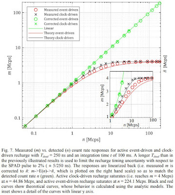
OSA Optics Express publishes a paper "Dynamic range extension for photon counting arrays" by Ivan Michel Antolovic, Claudio Bruschini, and Edoardo Charbon from TU Delft and EPFL.

"In this paper, we present a thorough analysis, which can actually be applied to any photon counting detector, on how to extend the SPAD dynamic range by exploiting the nonlinear photon response at high count rates and for different recharge mechanisms. We applied passive, active event-driven and clock-driven (i.e. clocked, following quanta image sensor response) recharge directly to the SPADs. The photon response, photon count standard deviation, signal-to-noise ratio and dynamic range were measured and compared to models. Measurements were performed with a CMOS SPAD array targeted for image scanning microscopy, featuring best-in-class 11 V excess bias, 55% peak photon detection probability at 520 nm and >40% from 440 to 640 nm. The array features an extremely low median dark count rate below 0.05 cps/μm2 at 9 V of excess bias and 0°C. We show that active event-driven recharge provides ×75 dynamic range extension and offers novel ways for high dynamic range imaging. When compared to the clock-driven recharge and the quanta image sensor approach, the dynamic range is extended by a factor of ×12.7-26.4. Additionally, for the first time, we evaluate the influence of clock-driven recharge on the SPAD afterpulsing."

Quanergy Troubles

Bloomberg reports about troubling signs at OPA-based LiDAR developer Quanergy that "has raised $160 million to date at a peak valuation of more than $1.5 billion."

"Quanergy has struggled to deliver products along the timelines it has set out for itself, and has shipped devices that don’t work as well as advertised. Numerous employees have left over the last 18 months, including several at key positions. But Quanergy’s biggest challenge is that its autonomous car business hasn’t developed the way it thought it would.

Quanergy has stopped talking about an IPO and has been pursuing new investments in recent months. It has had talks about finding a buyer, according to people with knowledge of the situation. Quanergy backers Samsung Ventures and Sensata Technologies Holding Plc, an auto sensor maker, have expressed disillusionment with the startup, according to people familiar with those firms.

Bloomberg also spoke to a half-dozen former employees, all of whom asked to remain anonymous, most of them citing the fear of retaliation. They said execution was a consistent problem at Quanergy. Several former employees described Eldada [the CEO] as a combustible and intimidating presence, stymying debate about product development and seeing any disagreement as intolerable dissent.

One former employee said he never saw a single device come off the line at Quanergy that met all of its stated specifications, an allegation the company denies.
"

The company CEO Louay Eldada publishes "Statement from Quanergy on Bloomberg Story" mostly denying Bloomberg analysis and conclusions.

Monday, August 13, 2018

MIT Time-Folded Optics Said to Offer New Possibilities

Optics.org: MIT Media Lab researches propose a new optics for fast cameras, say it adds new capabilities:

SmartSens Article Translation

SmartSens representative, The Hoffman Agency, kindly sent me a more correct translation of the company's article "Let China no longer miss the era of CIS." This comes to replace the half-broken Google translation in my previous post.

"Due to the late start and weak infrastructure of the semiconductor industry in China, the Chinese development of commercial CCD chips was completely buried and behind. The market used to be basically monopolized by Japanese manufacturers such as Sony, Panasonic and Sharp. Therefore, China completely missed the CCD era. With the rise of CIS, how to break the technology and market monopoly by Japanese and European manufacturers in the image sensor field has become the biggest challenge for the Chinese semiconductor industry.

Soon after graduating from the Hong Kong University of Science and Technology with his doctorate, Dr. Xu Chen went to Silicon Valley in the United States to pursue his own engineer dream. He joined the world's first company that launched commercial CIS chips, and engaged in the research and development of pixel components, the most important component in CIS development. During this time, Dr. Xu and his team developed and applied for nearly 30 patents. Since then, Dr. Xu has been engaged in technology research and development at leading CIS companies.

With the rise of Sony in the CIS field, the "Silicon Valley Power" has gradually declined, and "Asian Power" has risen to the front stage. It was at this time that Dr. Xu Chen first developed the idea of creating a Chinese brand to challenge the Japanese and European CIS giants.

In 2011, opportunities arose as China accelerated development in its tech industry. The central government introduced a series of policies designed to attract overseas talents, including the “Thousand Talents Plan.” Local governments also launched various policies to support the homecoming of oversea talents. It is at this prime time that Dr. Xu Chen returned to his motherland with his own visions, beliefs and core CIS innovations.

To Dr. Xu, successful Silicon Valley companies often share such characteristics: tech- and market-savvy founders, cohesive and go-getting teams, generous and people-oriented benefits, and compatible and diverse cultures. Not only has SmartSens, a company founded in China, inherited the Silicon Valley spirits from Dr. Xu Chen, but it continues to absorb globally educated talents to create a "Chinese core" in the CIS field. Founded on quality products and technological innovations, SmartSens is breaking the monopoly of Japanese and European manufacturers and leading China in the CIS era.
"

SmartSens founder Xu Chen

Sunday, August 12, 2018

Sharp ToF SPAD-based Proximity Sensor

Sharp and Socle/Foxconn come up with ST-like SPAD ToF proximity sensor, the MTOF171000C0. Sharp also makes a similar ToF proximity device, the GP2AP01VT10F, with quite a detailed spec. Application guide is available on Github. The samples are supposed to be available in August 2018.

Saturday, August 11, 2018

CMOSIS/Fillfactory Key Team Joins Gpixel

Gpixel: A team of CMOS image sensors industry veterans creates Gpixel NV. Gpixel NV is structured as a privately-held company and started operation on August 9th, 2018 providing turn-key solutions to industrial and professional markets ranging from sensor design, prototyping, characterization and packaging to qualification and volume production.

Gpixel NV founders are Tim Baeyens, Tim Blanchaert, Jan Bogaerts, Bart Ceulemans and Wim Wuyts. Together they have more than 75 person-years of relevant experience in CMOS imaging technology, development, operations and commercialization. Gpixel NV is set up with financial and operational backing of Gpixel Inc. (Gpixel Changchun Optotech), a CMOS sensor supplier based in Changchun, China, founded by Xinyang Wang in 2012.
Imaging and CMOS image sensors are ubiquitous today,” states Tim Baeyens, CEO of Gpixel NV. “Nevertheless, there is still a strong need for dedicated companies such as Gpixel to address high end markets like industrial and professional imaging. Through our wide industry network and strong collaboration with Gpixel Inc, we anticipate growing Gpixel rapidly to become one of the key players in solid state imaging.

Xinyang Wang, founder and CEO of Gpixel Inc. states, “I am very pleased to join forces with Gpixel NV to grow Gpixel to become a dominant player in our application areas. I am also convinced that the addition of Jan Bogaerts as Chief Technical Officer (CTO) and Wim Wuyts as Chief Commercial Officer (CCO) for Gpixel worldwide will foster our company’s innovation and global sales significantly.

Friday, August 10, 2018

Synaptics Rethinks its Under-Display Optical Fingerprint Business in Search for Better ROI

SeekingAlpha: Synaptics quarterly earnings call has interesting info on its optical under-display fingerprint sensor business:

"...we really take a big scrub on all of our products in the ROI and what provides the best investment going forward. And as we did that analysis, it was becoming clear ...that optical was going to be one of those boom and bust cycles. And to a certain degree, we lived through that with our capacitive solutions a few years back, and we did fantastic. But invariably, because it's somewhat of an optional solution and there's alternatives, it quickly went from a multi-dollar solution to a sub-$1 solution. And so, we enjoyed good money.

But if you look over the entire period, it wasn't the type of sticky highly differentiated business that we now seek as a company. And so, it would've taken additional investment or continued investment from our perspective. It somewhat hurts because we clearly were the innovators in the industry, and yes, we do see broader adoption of in-display fingerprint in the marketplace from a unit perspective and so on. But we can see the ASP erosion has begun, and there'll be multiple suppliers in it. Just from a long-term investment, we have better fish to fry right now. And so, it was purely an ROI decision.

...the revenues were fairly minimal. I'd say kind of in the sub $15 million to $20 million range is what's going away. We have bigger plans for it, as you saw at our Analyst Day, so we were expecting it to contribute about $100 million in fiscal 2019, and then more than that in fiscal 2020. But the actual impact year-over-year is fairly minimal at a Synaptics level.

...Now, that doesn't mean we're stopping. From the very beginning, when we went into this business, we said the ultimate solution was when fingerprint was truly integrated into the display. And eventually, when the market was right, we would have TDDI FP, so we're going to continue the investments in research in that particular area when we think the market might be ready, so you could have true in-display across the entire screen with multiple cost to the – minimal cost, excuse me, to the end user.
"

Thursday, August 9, 2018

Ouster on LiDAR Specmanship

Ouster presentation at Autonomous Vehicle Sensors Conference held in Jan Jose, CA in June 2018 defines the requirements to LiDARs and proposes their realistic measurement conditions, so that different products and technologies can be compared:


Links to few other interesting presentations at the conference:

- LiDAR for ADAS and Autonomous Driving by Hamamatsu
- AEye iDAR
- Frequency-Modulated Automotive Lidar by Blackmore
- Road to Robots by Yole
- Sony Automotive Sensors
- Camera-based Active Real-Time Driver Monitoring Systems by Seeing Machines

Himax Compares Smartphone ID Solutions, 3D Sensing

Himax quaterly earnings report presents the company's vision of 3D sensing market:

"Leading Android smartphone makers are exploring various 3D sensing technologies, namely structured light, active stereo camera (ASC) and, to a lesser extent, time-of-flight (ToF), trying to strike a good balance of cost, specifications and application. More software players are entering the ecosystem to develop 3D sensing applications beyond the existing applications, namely facial recognition, online payment and camera performance enhancement.

Himax has been working with an industry leading fingerprint solution provider to develop an under-display optical fingerprint product in the last two years, targeting smartphones using OLED displays. Himax provides a customized low-power image sensor in the solution. The Company is pleased to announce that the solution has entered into mass production with a major Android smartphone OEM for their new flagship model with shipment expected in the coming months. The CMOS image sensor used in the solution will have a notably higher ASP than the Company’s traditional display driver IC products.
"

SeekingAlpha: In Q&A session, Himax CEO Jordan Wu gives more details anout its optical fingerprint business:

"It appears to be to enjoy pretty good momentum right now in the Android market. Okay, because of cost issue. The business can change overnight in how they are, firstly, the cost, I’m talking about the total solution, which includes most importantly the CMOS image sensor, and as I said optics and certainly algorithm chip combined at the module. Initially, when the technology was promoted, we’re talking about $10 in total, but now, we are seeing $10 plus in total.

Now, we’re seeing the total cost is now coming down to $10 or even below. And because of certain cost saving measures adopted by module houses, in particular, in the optics side. So for that reason, again, customers want full screen design and they don’t want their capacity touch to be on the back, which is not convenient to use. So for full screen design, if you feel structured light too expensive, ToF is also quite expensive and even ASC is relatively expensive because ASC now, we’re still talking about $10 plus and this thing, fingerprint is already below $10.

So for that reason, it seems to be picking up momentum. However, I will have to say that the limitation of fingerprint is that it can do nothing out of the fingerprint, whether it’s all three kinds of 3D sensing, you can have a lot of other applications beyond unlocking your smartphone and payment. Right. So I think that is the most important thing. And certainly, under glass fingerprint, one reason why it is getting traction by it, it is not really becoming overwhelming. One of the issues is it still suffers from its lesser satisfactory accuracy, meaning when you try to unlock your phone, the failure rate still is too high. And when it fails, you have to – the user will have to key in the password, which people hate, right.

So in comparison, 3D sensing or face authentication, the accuracy level is a lot higher. And so they are certainly a big wildcard will be our first launch in expected September, right, in the new phones, whether they can introduce interesting attractive new features, application to 3D sensing. But I think it is still slightly too early to tell who is going to dominate which segment of the market as of today.
"

Wednesday, August 8, 2018

How to Bring CIS Industry to China

Update: The correct translation coming from the company representation is posted here. The one below is based on Google automatic one and is not accurate.

SmartSens Founder Xu Chen publishes an article on the company web site "Let China no longer miss the era of CIS." Few interesting quotes with help of Google translation:

"Due to the late start and poor foundation of Chinese semiconductors, the development of commercial CCD chips is completely behind the scenes. The market is basically monopolized by Japanese manufacturers such as Sony, Panasonic and Sharp, completely missing the CCD era. With the rise of CIS , how to break the technology and market monopoly of Japanese and European manufacturers in the field of image sensors has become a difficult problem for Chinese semiconductors.

In the year of graduation from Hong Kong University of Science and Technology, Dr. Xu Chen came to Silicon Valley in the United States with his own dream of engineers. He joined the world's first company to launch commercial CIS chips, and engaged in the research and development of pixel components , the most important component in CIS development. developed and applied for a close, during the 3 0 patents. Since then, Dr. Xu Chen has been engaged in technical development work at the CIS giant.

With the rise of Sony in the CIS field, the "Silicon Valley Power" has gradually declined, and "Asian Power" has entered the stage. It was at this time that Dr. Xu Chen first developed the idea of ​​creating a Chinese brand to challenge CIS Japanese and European giants.

In 2011 , it coincided with the introduction of a series of overseas talents introduction policies including the “Thousand Talents Plan” in order to accelerate the innovation of high-tech fields . Local governments also launched support policies to support the return of overseas talents. It is in this spring of the policy that Dr. Xu Chen returned to the motherland with his own ideals, beliefs and core CIS innovations.

Throughout Silicon Valley's successful innovation companies, they often have such characteristics — the founders who are proficient in technology and market-savvy, the united and powerful innovation team, the generous and people-oriented employee benefits, and the compatible and diverse corporate culture. The native of SmartSens only be obtained from Dr. Xu Chen from Silicon Valley, where such a temperament, but also has the world continue to absorb the educational background of creative talents, inclusive, and finally create a CIS in the field of "Chinese core" team, the quality of quality Based on the core of technological innovation, it has broken the monopoly of Japanese and European manufacturers, so that China will not miss the CIS era.
"

Tuesday, August 7, 2018

TPSCo Pixel Offerings

TowerJazz-Panasonic publishes the parameters of pixels it offers to its customers:

1.12μm-pixel 65nm CIS Platform

Global shutter pixel offerings (* means 4 additional masks for the designated pixel)

Update: TPSCo site has been changed on August 8, 2018, and more pixels are presented now: